Your new post is loading...
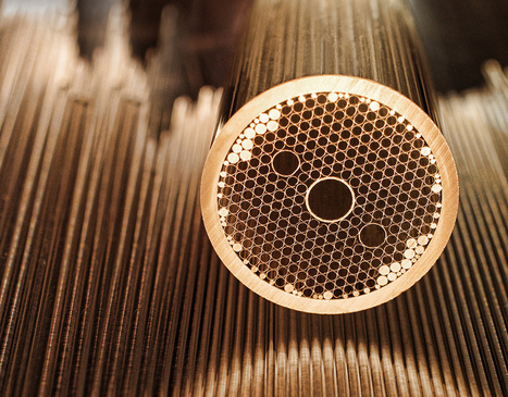
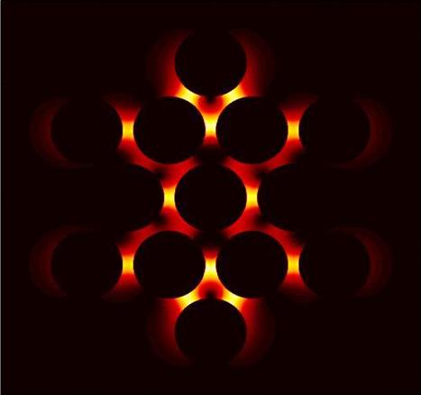
University of New Mexico researchers find decreasing the density of nanoparticles in ordered arrays produces exceptional field enhancements. Controlling the interactions between light and matter has been a long-standing ambition for scientists seeking to develop and advance numerous technologies that are fundamental to society. With the boom of nanotechnology in recent years, the nanoscale manipulation of light has become both, a promising pathway to continue this advancement, as well as a unique challenge due to new behaviors that appear when the dimensions of structures become comparable to the wavelength of light. Scientists in the Theoretical Nanophotonics Group at The University of New Mexico’s Department of Physics and Astronomy have made an exciting new advancement to this end, in a pioneering research effort titled “Analysis of the Limits of the Near-Field Produced by Nanoparticle Arrays,” published recently in the journal, ACS Nano, a top journal in the field of nanotechnology. The group, led by Assistant Professor Alejandro Manjavacas, studied how the optical response of periodic arrays of metallic nanostructures can be manipulated to produce strong electric fields in their vicinity. The arrays they studied are composed of silver nanoparticles, tiny spheres of silver that are hundreds of times smaller than the thickness of a human hair, placed in a repeating pattern, though their results apply to nanostructures made of other materials as well. Because of the strong interactions between each of the nanospheres, these systems can be used for different applications, ranging from vivid, high-resolution color printing to biosensing that could revolutionize healthcare.
Using a layer of self-assembled particles allows researcher to etch an almost-perfect reflector. Using a metamaterial created out of silicon, scientists have created a way to create an almost-perfect reflector that would be used for lasers and telescopes. The world has become increasingly fascinated with worlds beyond our own, more so, the cosmos. To get a better understanding of the stars and planets/exoplanets near and far, scientists require the best telescopes that will reflect perfect light. Recently published in ACS Photonics of 8 May 2015, advantages have been taken from dielectric metamaterials than plasmonic materials because it offers low-loss alternatives. With the help of this material and the focus on an alternative method, it helps separate the electric and magnetic resonances to achieve the required reflection bandwidth while maintaining high tolerance to disorder. In other words, the material helps produce a sharper more accurate reflection while allowing scientists to scan different bandwidths with ease, with high resolution and very very minimal loss.
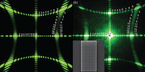
Scientists from Russia and Australia have put forward a simple new way of counting microscopic particles in optical materials by means of a laser. A light beam passing through such a material splits and forms a characteristic pattern consisting of numerous bright spots on a projection screen. The researchers found that the number of these spots corresponds exactly to the number of scattering microscopic particles in the optical material. Therefore, the structure and shape of any optical material can be determined without resorting to the use of expensive electron or atomic-force microscopy. According to the researchers, the new method will help design optical devices much faster. The work was published in Scientific Reports. The production of optical circuits requires devices that can amplify optical signals, bring them into focus, rotate and change their type of motion. Ordinary lenses cannot cope with these tasks at nanoscale, so scientists are working with artificial optical materials - photonic crystals and metamaterials, which can control the propagation of light in most extraordinary ways. However, fabricating optical materials with desired properties is a laborious process that needs constant improvement. The scientists from ITMO University, Ioffe Institute, and Australian National University for the first time suggested analyzing the structure of photonic crystals using optical diffraction method, that is, by looking at the light pattern generated while the sample is exposed to a laser beam. The study has shown that the number of these spots is equal to the number of scattering microscopic particles in the sample structure. Previously, such small particles could only be seen and counted with powerful and expensive electron or atomic-force microscopes. "The light senses heterogeneity," says Mikhail Rybin, first author of the paper, senior researcher at the Department of Nanophotonics and Metamaterials at ITMO University.
Via Mariaschnee
Tufts University biomedical engineers are using low-energy, ultrafast laser technology to make high-resolution, 3-D structures in silk protein hydrogels. The laser-based micropatterning represents a new approach to customized engineering of tissue and biomedical implants.
The work is reported in a paper in PNAS Early Edition published September 15 online before print: "Laser-based three-dimensional multiscale micropatterning of biocompatible hydrogels for customized tissue engineering scaffolds."
Artificial tissue growth requires pores, or voids, to bring oxygen and nutrients to rapidly proliferating cells in the tissue scaffold. Current patterning techniques allow for the production of random, micron-scale pores and the creation of channels that are hundreds of microns in diameter, but there is little in between.
The Tufts researchers used an ultrafast, femtosecond laser to generate scalable, high-resolution 3-D voids within silk protein hydrogel, a soft, transparent biomaterial that supports cell growth and allows cells to penetrate deep within it. The researchers were able to create voids at multiple scales as small as 10 microns and as large at 400 microns over a large volume.
Further, the exceptional clarity of the transparent silk gels enabled the laser's photons to be absorbed nearly 1 cm below the surface of the gel – more than 10 times deeper than with other materials, without damaging adjacent material.
The laser treatment can be done while keeping the cell culture sealed and sterile. Unlike most 3-D printing, this technique does not require photoinitiators, compounds that promote photoreactivity but are typically bio-incompatible.
"Because the femtosecond laser pulses allow us to target specific regions without any damage to the immediate surroundings, we can imagine using such micropatterning to controllably design around living cells, guide cell growth and create an artificial vasculature within an already densely seeded silk hydrogel," said senior author Fiorenzo G. Omenetto, Ph.D. Omenetto is associate dean for research, professor of biomedical engineering and Frank C. Doble professor at Tufts School of Engineering and also holds an appointment in physics in the School of Arts and Sciences.
Most lenses are, by definition, curved. After all, they are named for their resemblance to lentils, and a glass lens made flat is just a window with no special powers. But a new type of lens created at the Harvard School of Engineering and Applied Sciences(SEAS) turns conventional optics on its head.
A major leap forward from a prototype device demonstrated in 2012, it is an ultra-thin, completely flat optical component made of a glass substrate and tiny, light-concentrating silicon antennas. Light shining on it bends instantaneously, rather than gradually, while passing through. The bending effects can be designed in advance, by an algorithm, and fine-tuned to fit almost any purpose.
With this new invention described today in Science, the Harvard research team has overcome an inherent drawback of a wafer-thin lens: light at different wavelengths (i.e., colors) responds to the surface very differently. Until now, this phenomenon has prevented planar optics from being used with broadband light. Now, instead of treating all wavelengths equally, the researchers have devised a flat lens with antennas that compensate for the wavelength differences and produce a consistent effect—for example, deflecting three beams of different colors by the same angle, or focusing those colors on a single spot.
“What this now means is that complicated effects like color correction, which in a conventional optical system would require light to pass through several thick lenses in sequence, can be achieved in one extremely thin, miniaturized device,” said principal investigator Federico Capasso, the Robert L. Wallace Professor of Applied Physics and Vinton Hayes Senior Research Fellow in Electrical Engineering at Harvard SEAS.
Watching a movie played in reverse often makes us laugh because unexpected and mysterious things seem to happen: glass shards lying on the floor slowly start to move towards each other, magically assemble and suddenly an intact glass jumps on the table where it gently gets to a halt. Or snow starts to from a water puddle in the sun, steadily growing until an entire snowman appears as if molded by an invisible hand. When we see such scenes, we immediately realize that according to our everyday experience something is out of the ordinary. Indeed, there are many processes in nature that can never be reversed. The physical law that captures this behavior is the celebrated second law of thermodynamics, which posits that the entropy of a system – a measure for the disorder of a system – never decreases spontaneously, thus favoring disorder (high entropy) over order (low entropy).
However, when we zoom into the microscopic world of atoms and molecules, this law softens up and looses its absolute strictness. Indeed, at the nanoscale the second law can be fleetingly violated. Recently, a team of physicists of the University of Vienna, the Institute of Photonic Sciences in Barcelona and the Swiss Federal Institute of Technology in Zürich succeeded in accurately predicting the likelihood of events transiently violating the second law of thermodynamics. They immediately put the mathematical fluctuation theorem they derived to the test using a tiny glass sphere with a diameter of less than 100 nm levitated in a trap of laser light. Their experimental set-up allowed the research team to capture the nano-sphere and hold it in place, and, furthermore, to measure its position in all three spatial directions with exquisite precision. In the trap, the nano-sphere rattles around due to collisions with surrounding gas molecules. By a clever manipulation of the laser trap the scientists cooled the nano-sphere below the temperature of the surrounding gas and, thereby, put it into a non-equilibrium state. They then turned off the cooling and watched the particle relaxing to the higher temperature through energy transfer from the gas molecules. The researchers observed that the tiny glass sphere sometimes, although rarely, does not behave as one would expect according to the second law: the nano-sphere effectively releases heat to the hotter surroundings rather than absorbing the heat. The theory derived by the researchers to analyze the experiment confirms the emerging picture on the limitations of the second law on the nanoscale.
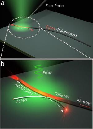
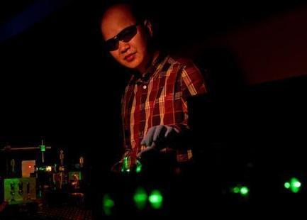
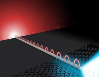
Recently, researchers have been developing a new type of laser that combines photons and plasmons (electron density oscillations) into a single radiation-emitting device with unique properties. The hybrid photon-plasmon nanowire laser is composed of a Ag nanowire and a CdSe nanowire coupled into an X-shape. This type of coupling enables the photonic and plasmonic modes to be separated, which gives the hybrid laser advantageous features.
"Compared to conventional photon lasers, the hybrid photon-plasmon nanowire laser offers two outstanding possibilities: the extremely thin laser beam (e.g., down to the size of a single molecule) and the ultrafast modulation (e.g., >THz repetition rate), both stemming from the longitudinally separable pure plasmon nanowire mode," Limin Tong, Professor at Zhejiang University in Hangzhou China, told Phys.org. "Owing to the above-mentioned merits, photon-plasmon lasers are potentially better for certain applications such as strong coupling of quantum nanoemitters, ultra-sensitivity optical sensing, and ultrafast-modulated coherent sources."
In a new study, the researchers have demonstrated that the photon and plasmon nanowire waveguides can be coupled in the longitudinal direction; that is, along the direction of the beams. This type of coupling makes it possible to spatially separate the plasmonic mode from the photonic mode, and to simultaneously use both modes. Under excitation, strong luminous spots are observed at both ends of the hybrid cavity, with interference rings indicating strong spatial coherence of the light emitted. The output spot of the Ag nanowire is much smaller than that of the CdSe nanowire, indicating much tighter confinement of the plasmon radiation.
The advantages of ultratight confinement and ultrafast modulation offered by side-coupling a plasmonic nanowire waveguide to a photonic one enable the hybrid laser to provide very precise lasing, which could be delivered to very small areas such as quantum dots. Photon-plasmon lasers can also have applications for nanophotonic circuits, biosensing, and quantum information processing. The researchers plan to make further improvements to the laser in the future. "One of our future plans is to introduce the ultrafast nonlinear effects of the plasmonic nanowire into the hybrid laser, and explore the possibility of ultrafast-modulation of the nanolaser, while offering a far-field-accessible pure plasmon cavity mode with sub-diffration-limited beam size," Tong said.
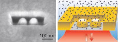
A single cell in our body is composed of thousands of millions of different biomolecules that work together in an extremely well-coordinated way. Likewise, many biological and biochemical reactions occur only if molecules are present at very high concentrations. Understanding how all these molecules interact with each other is key to advancing our knowledge in molecular and cell biology. This knowledge is of central and fundamental importance in the quest for the detection of the earliest stages of many human diseases. As such, one of ultimate goals in Life Sciences and Biotechnology is to observe how individual molecules work and interact with each other in these very crowded environments. Unfortunately, detecting one molecule amongst millions of neighbouring molecules has been technically impossible until now. The key to successfully detecting the single molecule lies in the conception and production of a working device that shrinks the observation region to a tiny size that is comparable to the size of the molecule itself, i.e. only a few nanometres. Researchers at the Fresnel Institute in Marseille and ICFO-the Institute for Photonic Sciences in Barcelona report in Nature Nanotechnology the design and fabrication of the smallest optical device, capable of detecting and sensing individual biomolecules at concentrations that are similar to those found in the cellular context. The device called "antenna-in-a-box" consists on a tiny dimer antenna made out of two gold semi-spheres, separated from each other by a gap as small as 15nm. Light sent to this antenna is enormously amplified in the gap region where the actual detection of the biomolecule of interest occurs. Because amplification of the light is confined to the dimensions of the gap, only molecules present in this tiny region are detected. A second trick that the researchers used to make this device work was to embed the dimer antennas inside boxes also of nanometric dimensions. "The box screens out the unwanted "noise" of millions of other surrounding molecules, reducing the background and improving as a whole the detection of individual biomolecules.", explains Jerome Wenger from Fresnel Institute. When tested under different sample concentrations, this novel antenna-in-box device allowed for 1100-fold fluorescence brightness enhancement together with detection volumes down to 58 zeptoliters (1 zL = 10E-21L), i.e., the smallest observation volume in the world. The antenna-in-a-box offers a highly efficient platform for performing a multitude of nanoscale biochemical assessments with single molecule sensitivity at physiological conditions. It could be used for ultrasensitive sensing of minute amounts of molecules, becoming an excellent early diagnosis device for biosensing of many disease markers. "It can also be used as an ultra-bright optical nanosource to illuminate molecular processes in living cells and ultimately visualize how individual biomolecules interact with each other. This brings us closer to the long awaited dream of biologists", concludes ICFO researcher Prof. Maria Garcia-Parajo.
Computers may be getting faster every year, but those advances in computer speed could be dwarfed if their 1’s and 0’s were represented by bursts of light, instead of electricity. Researchers at the University of Pennsylvania have made an important advance in this frontier of photonics, fashioning the first all-optical photonic switch out of cadmium sulfide nanowires. Moreover, they combined these photonic switches into a logic gate, a fundamental component of computer chips that process information. The research team began by precisely cutting a gap into a nanowire. They then pumped enough energy into the first nanowire segment that it began to emit laser light from its end and through the gap. Because the researchers started with a single nanowire, the two segment ends were perfectly matched, allowing the second segment to efficiently absorb and transmit the light down its length. “Putting switches together lets you make logic gates, and assembling logic gates allows you to do computation,” Piccione said. “We used these optical switches to construct a NAND gate, which is a fundamental building block of modern computer processing.” “We see a future where ‘consumer electronics’ become ‘consumer photonics".
Electrical engineers at The University of Texas at Arlington and at the University of Wisconsin-Madison have devised a new laser for on-chip optical connections that could give computers a huge boost in speed and energy efficiency. At just 2 micrometers in height — smaller than the width of a human hair — the surface-emitting laser's vastly lower profile could make it cheaper and easier for manufacturers to integrate high-speed optical data connections into the microprocessors powering the next generation of computers.
Engineers at Brown University and QD Vision Inc. have created nanoscale single crystals that can produce the red, green, or blue laser light needed in digital displays. The size determines color, but all the pyramid-shaped quantum dots are made the same way of the same elements. In experiments, light amplification required much less power than previous attempts at the technology. The team’s prototypes are the first lasers of their kind.
|
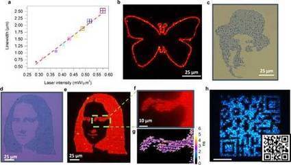
The use of quantum dots (QDs) in practical applications relies on the ability to precisely pattern QDs on substrates with desired optical properties. Typical direct-write printing techniques such as inkjet and gravure printing are limited in resolution (micron-scale), structural complexity, and require significant post-processing time.In new work, researchers at the University of Texas at Austin use laser-induced bubble printing to pattern CdSe/CdS QDs on plasmonic substrates with submicron resolution (<700nm line width), high throughput (∼10E4 µm/s) and strong QD-substrate adhesion.Not only is the bubble-mediated immobilization at the submicron scale stable, but the submicron-sized bubble's stability can be maintained over a large area. This technique is also compatible with flexible substrates and can be further integrated with smartphone to realize haptic integration. Finally, the emission characteristics of the QDs in terms of the emission wavelength and lifetime can be modified in real-time to achieve site-sensitive emission.The team, led by Yuebing Zheng, Assistant Professor of Mechanical Engineering and Materials Science & Engineering has been published in ACS Applied Materials & Interfaces ("High-Resolution Bubble Printing of Quantum Dots").
Light, when strongly concentrated, is enormously powerful. Now, a team of physicists led by Professor Jörg Schreiber from the Institute of Experimental Physics – Medical Physics, which is part of the Munich-Centre for Advanced Photonics (MAP), a Cluster of Excellence at LMU Munich, has used this energy source with explosive effect. The researchers focus high-power laser light onto beads of plastic just a few micrometers in size. The concentrated energy blows the nanoparticles apart, releasing radiation made up of positively charged atoms (protons). Such proton beams could be used in future for treating tumors, and in advanced imaging techniques. Their findings appear in the journal Physical Review E.
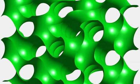
"A team of researchers with Swinburne University of Technology in Australia has found a way to use two-beam super-resolution lithography to create 3D photonic "gyroid" nanostructures—similar to those found in butterfly wings. In their paper published in the journal Science Advances, the team describes their technique and some applications to which it might be applied.
Scientists have known for some time that butterfly wings have "gyroid" nanostructures in them (arranged in grid patterns), that serve the butterflies by manipulating light in useful ways. In addition to their photonic properties, the structures, which are made of intertwining curved surfaces, were also found to be very strong for their size, which has caused scientists to see if they might find a way to create them artificially. Up till now, such efforts have left a lot to be desired—most do not have a high enough resolution or are too fragile. In this new effort, the researchers report that rather than rely on traditional methods, such as two-photon polymerization, the team went with optical two-beam super-resolution lithography—they compare it to direct laser writing techniques, noting that it has two major advantages over other techniques used in the past. The first is that it offers much better resolution and the second is that the resulting structure has more mechanical strength."
Via Mariaschnee
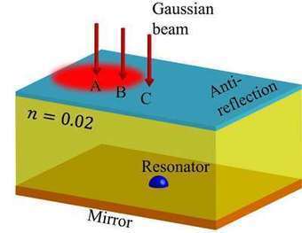
University of Wisconsin-Madison engineers have created a nanoscale device that can emit light as powerfully as an object 10,000 times its size. It's an advance that could have huge implications for a variety of imaging and energy applications.
In a paper published July 10, 2015 in the journal Physical Review Letters, Zongfu Yu, an assistant professor of electrical and computer engineering at UW-Madison, and his collaborators describe nanoscale device that that drastically outpaces previous technology in its ability to scatter light. They showed how a single nanoresonator can manipulate light to cast a very large "reflection." The nanoresonator's capacity to absorb and emit light energy is such that it can make itself—and, in applications, other very small things—appear 10,000 times as large as its physical size.
"Making an object look much 10,000 times larger than its physical size has lots of implications in technologies related to light," Yu says. The researchers realized the advance through materials innovation and a keen understanding of the physics of light. Much like sound, light can resonate, amplifying itself as the surrounding environment manipulates the physical properties of its wave energy. The researchers took advantage of this by creating an artificial material in which the wavelength of light is much larger than in a vacuum, which allows light waves to resonate more powerfully.
In a paper published July 10, 2015 in the journal Physical Review Letters, Zongfu Yu, an assistant professor of electrical and computer engineering at UW-Madison, and his collaborators describe nanoscale device that that drastically outpaces previous technology in its ability to scatter light. They showed how a single nanoresonator can manipulate light to cast a very large "reflection."
The nanoresonator's capacity to absorb and emit light energy is such that it can make itself—and, in applications, other very small things—appear 10,000 times as large as its physical size.
"Making an object look much 10,000 times larger than its physical size has lots of implications in technologies related to light," Yu says. The researchers realized the advance through materials innovation and a keen understanding of the physics of light. Much like sound, light can resonate, amplifying itself as the surrounding environment manipulates the physical properties of its wave energy. The researchers took advantage of this by creating an artificial material in which the wavelength of light is much larger than in a vacuum, which allows light waves to resonate more powerfully.
Scientists at the University of Rochester and Swiss Federal Institute of Technology in Zurich have devised an experimental circuit consisting of a silver nanowire and a single-layer atomically thin flake of molybendum disulfide (MoS2) — a step toward building computer chips capable of transporting digital information at light speed.
The researchers used a laser to excite electromagnetic waves called plasmons (vibrating electron clouds) at the surface of the wire, causing an MoS2 flake at the far end of the wire to generate strong light emission. MoS2 excitons can also decay into nanowire plasmons, they found.
This interaction an be exploited for creating nanophotonic integrated circuits, said Nick Vamivakas, assistant professor of quantum optics and quantum physics at the University of Rochester and senior author of the paper in the journal Optica.
Photonic devices can be much faster than electronic ones, but they are bulkier and cannot be miniaturized nearly as well as electronic circuits. The new results hold promise for guiding the transmission of light and maintaining the intensity of the signal in very small dimensions.
In bulk MoS2, electrons and photons interact as they would in traditional semiconductors like silicon and gallium arsenide. But when MoS2 is trimmed down to an atomically thin layer, the transfer of energy between electrons and photons becomes highly efficient.*
Combining electronics and photonics on the same integrated circuits could drastically improve the performance and efficiency of mobile technology. The researchers say the next step is to create a near-field detector based on MoS2 and an MoS2 light-emitting diode coupled to on-chip nanoplasmonic circuitry.
* The key to MoS2′s desirable photonic properties is in the structure of its energy band gap. As the material’s layer count decreases, it transitions from an indirect to direct band gap, which allows electrons to easily move between energy bands by releasing photons. Graphene is inefficient at light emission because it has no band gap.
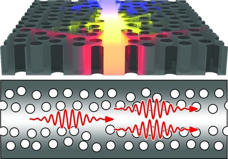
Researchers the world round are working to develop optical chips, where light can be controlled with nanostructures. These could be used for future circuits based on light (photons) instead of electron - that is photonics instead of electronics. But it has proved to be impossible to achieve perfect photonic nanostructures: they are inevitably a little bit imperfect. Now researchers at the Niels Bohr Institute in collaboration with DTU have discovered that imperfect nanostructures can offer entirely new functionalities. They have shown that imperfect optical chips can be used to produce 'nanolasers', which is an ultimately compact and energy-efficient light source. The results are published in the scientific journal Nature Nanotechnology.
The researchers are working with extremely small photonic crystal membranes - the width of the membrane is 25 micrometer, and the thickness is 340 nanometers (1 nanometer is one thousandth of a micrometer). The crystals are made of the semiconducting material gallium arsenide (GaAs). A pattern of holes are etched into the material at a regular distance of 380 nanometers. The holes have the function of acting as built-in mirrors that reflect the light and can thus be used to control the spread of the light in the optical chip. The researchers have therefore tried to achieve as perfect a regular structure of holes as possible to control the light in certain optical circuit.
"It turns out that the imperfect optical chips are extremely well suited for capturing light. When the light is sent into the imperfect chip, it will hit the many small irregular holes, which reflect the light in random directions. Due to the frequent reflections, the light is spontaneously captured in the nanostructure and cannot escape. This allows the light to be amplified, resulting in surprisingly good conditions for creating highly efficient and compact lasers," explains Peter Lodahl, professor and head of the Quantum Photonic research group at the Niels Bohr Institute at the University of Copenhagen.
Researchers at MIT have proposed a new system that combines ferroelectric materials — the kind often used for data storage — with graphene, a two-dimensional form of carbon known for its exceptional electronic and mechanical properties. The resulting hybrid technology could eventually lead to computer and data-storage chips that pack more components in a given area and are faster and less power-hungry.
The new system works by controlling waves called surface plasmons. These waves are oscillations of electrons confined at interfaces between materials; in the new system the waves operate at terahertz frequencies. Such frequencies lie between those of far-infrared light and microwave radio transmissions, and are considered ideal for next-generation computing devices.
The team’s new system allows waves to be concentrated at much smaller length scales, which could lead to a tenfold gain in the density of components that could be placed in a given area of a chip, Fang says.
The team’s initial proof-of-concept device uses a small piece of graphene sandwiched between two layers of the ferroelectric material to make simple, switchable plasmonic waveguides. This work used lithium niobate, but many other such materials could be used, the researchers say.
Light can be confined in these waveguides down to one part in a few hundreds of the free-space wavelength, Jin says, which represents an order-of-magnitude improvement over any comparable waveguide system. “This opens up exciting areas for transmitting and processing optical signals,” he says.
Rice University scientists have unveiled a robust new method for arranging metal nanoparticles in geometric patterns that can act as optical processors that transform incoming light signals into output of a different color. Rice's team used the method to create an optical device in which incoming light could be directly controlled with light via a process known as "four-wave mixing." Four-wave mixing has been widely studied, but Rice's disc-patterning method is the first that can produce materials that are tailored to perform four-wave mixing with a wide range of colored inputs and outputs. "Versatility is one of the advantages of this process," said study co-author Naomi Halas, director of LANP and Rice's Stanley C. Moore Professor in Electrical and Computer Engineering and a professor of biomedical engineering, chemistry, physics and astronomy. "It allows us to mix colors in a very general way. That means not only can we send in beams of two different colors and get out a third color, but we can fine-tune the arrangements to create devices that are tailored to accept or produce a broad spectrum of colors." The information processing that takes place inside today's computers, smartphones and tablets is electronic. Each of the billions of transistors in a computer chip uses electrical inputs to act upon and modify the electrical signals passing through it. Processing information with light instead of electricity could allow for computers that are both faster and more energy-efficient, but building an optical computer is complicated by the quantum rules that light obeys.
With laser beams, molecules can be fixed at exactly the right position in a three dimensional material. The new method can be used to grow biological tissue or to create micro sensors. "3-D-photografting" is the name of the new method. Two research teams from the Vienna University of Technology collaborated closely to develop it: Professor Jürgen Stampfl's materials science team and Professor Robert Liska's research group for macromolecular chemistry. Both research groups have already attracted considerable attention in the past, developing new kinds of 3-D-printers. When biological tissue is grown, this method can allow the positioning of chemical signals, telling living cells where to attach. The new technique also holds promise for sensor technology: A tiny three dimensional "lab on a chip" could be created, in which accurately positioned molecules react with substances from the environment. The scientists start with a so-called hydrogel -- a material made of macromolecules, arranged in a loose meshwork. Between those molecules, large pores remain, through which other molecules or even cells can migrate. Specially selected molecules are introduced into the hydrogel meshwork, then certain points are irradiated with a laser beam. At the positions where the focused laser beam is most intense, a photochemically labile bond is broken. That way, highly reactive intermediates are created which locally attach to the hydrogel very quickly. The precision depends on the laser's lens system, at the Vienna University of Technology a resolution of 4 µm could be obtained. Depending on the application, different molecules can be used. 3-D photografting is not only useful for bio-engineering but also for other fields, such as photovoltaics or sensor technology. In a very small space, molecules can be positioned which attach to specific chemical substances and allow their detection. A microscopic three-dimensional "lab on a chip" becomes possible.
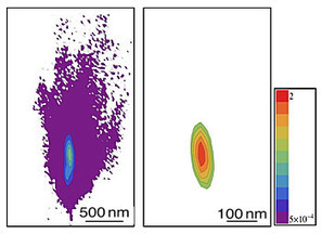
NIST researchers’ new approach to trapping nanoparticles uses a control and feedback system that nudges them only when needed, lowering the average intensity of the beam and increasing the lifetime of the nanoparticles while reducing their tendency to wander. In the picture on the left, 100-nanometer gold nanoparticles quickly escape from a static trap while gold nanoparticles trapped using the NIST method remained strongly confined. Scientists routinely trap and move nanoparticles in a solution with "optical tweezers"—a laser focused to a very small point. The tiny dot of laser light creates a strong electric field, or potential well, that attracts particles to the center of the beam. Although the particles are attracted into the field, the molecules of the fluid they are suspended in tend to push them out of the well. This effect only gets worse as particle size decreases because the laser's influence over a particle's movement gets weaker as the particle gets smaller. One can always turn up the power of the laser to generate a stronger electric field, but doing that can fry the nanoparticles too quickly to do anything meaningful with them—if it can hold them at all. Using a refined technique for trapping and manipulating nanoparticles, researchers at the National Institute of Standards and Technology (NIST) have extended the trapped particles' useful life more than tenfold.* This new approach, which one researcher likens to "attracting moths," promises to give experimenters the trapping time they need to build nanoscale structures and may open the way to working with nanoparticles inside biological cells without damaging the cells with intense laser light.
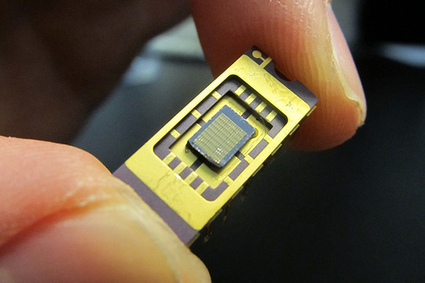
A new ultrafast, nanoscale light-emitting diode (LED) device developed at Stanford’s School of Engineering transmits data at ultrafast rates while using 2,000 times less energy than laser-based systems in use today,” The nanophotonic device is a major step forward for on-chip data transmission, the researchers say. The device can transmit data at 10 gigabits per second. The researchers say it is a major step forward in providing a practical ultrafast, low-power, room-temperature light source for on-chip data transmission.
|